Author Affiliations
Abstract
National Key Laboratory of Solid-State Microwave Devices and Circuits, Hebei Semiconductor Research Institute, Shijiazhuang 050051, China
In this letter, high power density AlGaN/GaN high electron-mobility transistors (HEMTs) on a freestanding GaN substrate are reported. An asymmetric Γ-shaped 500-nm gate with a field plate of 650 nm is introduced to improve microwave power performance. The breakdown voltage (BV) is increased to more than 200 V for the fabricated device with gate-to-source and gate-to-drain distances of 1.08 and 2.92 μm. A record continuous-wave power density of 11.2 W/mm@10 GHz is realized with a drain bias of 70 V. The maximum oscillation frequency (fmax) and unity current gain cut-off frequency (ft) of the AlGaN/GaN HEMTs exceed 30 and 20 GHz, respectively. The results demonstrate the potential of AlGaN/GaN HEMTs on free-standing GaN substrates for microwave power applications.
freestanding GaN substrates AlGaN/GaN HEMTs continuous-wave power density breakdown voltage Γ-shaped gate Journal of Semiconductors
2024, 45(1): 012501
1 中国电子科技集团公司第十三研究所, 河北石家庄 050051
2 固态微波器件与电路全国重点实验室, 河北石家庄 050051
介绍了一款基于 GaAs肖特基二极管单片工艺的 220 GHz倍频器的设计过程以及测试结果。为提高输出功率, 倍频器采用多阳极结构, 8个二极管在波导呈镜像对称排列, 形成平衡式倍频器结构。采用差异式结电容设计解决了多阳极结构端口散射参数不一致问题, 提高了倍频器的转换效率和工作带宽。对设计的倍频器进行流片、装配和测试, 测试结果显示: 倍频器在 204~ 234 GHz频率范围内, 转化效率大于 15%; 226 GHz峰值频率下实现最大输出功率为 90.5 mW, 转换效率为 22.6%。设计的 220 GHz倍频器输出功率高, 转化效率高, 工作带宽大。
倍频器 太赫兹 肖特基二极管 结电容 单片 frequency doubler tearhertz Schottky barrier diode junction capacitance Microwave Monolithic Integrated Circuit 太赫兹科学与电子信息学报
2023, 21(9): 1080
1 重庆邮电大学 光电工程学院, 重庆 400065
2 重庆光电技术研究所, 重庆 400060
3 重庆邮电大学 通信与信息工程学院, 重庆 400065
4 中国电子科技集团第十三研究所, 石家庄 050057
5 暨南大学 纳米光子学研究院, 广州 511443
设计了一种基于双十字结构的多谐振峰太赫兹超材料传感器。整体结构由表面金属图案、中间介质和底面金属板组成。基本单元的表面图案呈双十字交叉状,介质材料为聚酰亚胺(Polyimide)。仿真结果表明,所提出的结构具有5个不同的谐振吸收峰,吸收率均超过90%。前3个谐振峰分别对应单元结构内部不同区域形成的基本磁谐振,后2个谐振峰则来源于单元结构间的相互作用。当传感器表面覆盖15μm厚的分析物时,该传感器各个谐振峰的灵敏度分别为72,137,234,353和252GHz/RIU,且谐振峰偏移量与待测分析物折射率变化量呈较强的线性关系,具有优越的传感特性。此外,多峰传感器稳定性优于传统的单峰或双峰传感器,具有良好的抗干扰能力,有助于降低测量误差。所提出的这种高灵敏度多谐振峰传感器在微量分子检测领域具有广阔的应用前景。
太赫兹 超材料 传感器 多谐振峰 灵敏度 terahertz metamaterial sensor multiple resonance peaks sensitivity

Author Affiliations
Abstract
National Key Laboratory of ASIC, Hebei Semiconductor Research Institute, Shijiazhuang 050051, China
In this work, high-stability 4H-SiC avalanche photodiodes (APDs) for ultraviolet (UV) detection at high temperatures are fabricated and investigated. With the temperature increasing from room temperature to 150°C, a very small temperature coefficient of 7.4 mV/°C is achieved for the avalanche breakdown voltage of devices. For the first time, the stability of 4H-SiC APDs is verified based on an accelerated aging test with harsh stress conditions. Three different stress conditions are selected with the temperatures and reverse currents of 175°C/100 µA, 200°C/100 µA, and 200°C/500 µA, respectively. The results show that our 4H-SiC APD exhibits robust high-temperature performance and can even endure more than 120 hours at the harsh aging condition of 200°C/500 µA, which indicates that 4H-SiC APDs are very stable and reliable for applications at high temperatures.
silicon carbide photodiode UV detector high temperature avalanche Geiger mode Chinese Optics Letters
2023, 21(3): 032502

Author Affiliations
Abstract
National Key Laboratory of Application Specific Integrated Circuit (ASIC), Hebei Semiconductor Research Institute, Shijiazhuang 050051, China
Ga2O3 metal–oxide–semiconductor field-effect transistors (MOSFETs) with high-breakdown characteristics were fabricated on a homoepitaxial n-typed β-Ga2O3 film, which was grown by metal organic chemical vapor deposition (MOCVD) on an Fe-doped semi-insulating (010) Ga2O3 substrate. The structure consisted of a 400 nm unintentionally doped (UID) Ga2O3 buffer layer and an 80 nm Si-doped channel layer. A high k HfO2 gate dielectric film formed by atomic layer deposition was employed to reduce the gate leakage. Moreover, a source-connected field plate was introduced to enhance the breakdown characteristics. The drain saturation current density of the fabricated device reached 101 mA/mm at Vgs of 3 V. The off-state current was as low as 7.1 × 10⁻¹¹ A/mm, and the drain current ION/IOFF ratio reached 109. The transistors exhibited three-terminal off-state breakdown voltages of 450 and 550 V, corresponding to gate-to-drain spacing of 4 and 8 μm, respectively.
Journal of Semiconductors
2019, 40(1): 012803

Author Affiliations
Abstract
National Key Laboratory of ASIC, Hebei Semiconductor Research Institute, Shijiazhuang 050051, China
Ultraviolet (UV) detectors with large photosensitive areas are more advantageous in low-level UV detection applications. In this Letter, high-performance 4H-SiC p-i-n avalanche photodiodes (APDs) with large active area (800 μm diameter) are reported. With the optimized epitaxial structure and device fabrication process, a high multiplication gain of 1.4 × 10⁶ is obtained for the devices at room temperature, and the dark current is as low as ~10 pA at low reverse voltages. In addition, record external quantum efficiency of 85.5% at 274 nm is achieved, which is the highest value for the reported SiC APDs. Furthermore, the rejection ratio of UV to visible light reaches about 104. The excellent performance of our devices indicates a tremendous improvement for large-area SiC APD-based UV detectors. Finally, the UV imaging performance of our fabricated 4H-SiC p-i-n APDs is also demonstrated for system-level applications.
040.1345 Avalanche photodiodes (APDs) 040.7190 Ultraviolet 040.6070 Solid state detectors 230.5160 Photodetectors Chinese Optics Letters
2019, 17(9): 090401
Author Affiliations
Abstract
National Key Laboratory of ASIC, Hebei Semiconductor Research Institute, Shijiazhuang 050051, China
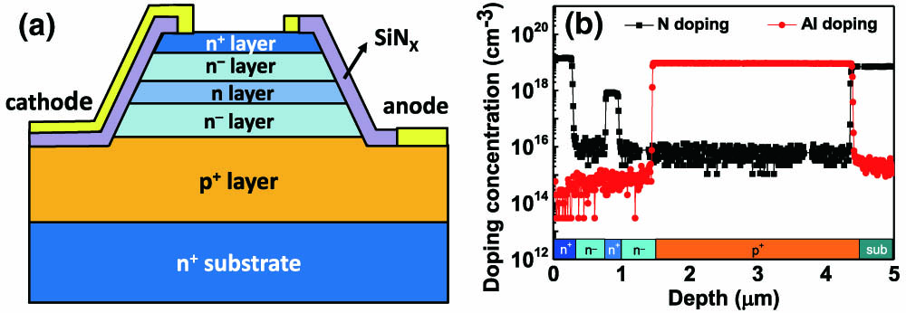
In this Letter, we report large-area (600 μm diameter) 4H-SiC avalanche photodiodes (APDs) with high gain and low dark current for visible-blind ultraviolet detection. Based on the separate absorption and multiplication structure, 4H-SiC APDs passivated with SiNx instead of SiO2 are demonstrated for the first time, to the best of our knowledge. Benefitting from the SiNx passivation, the surface leakage current is effectively suppressed. At room temperature, high multiplication gain of 6.5×10⁵ and low dark current density of 0.88 μA/cm2 at the gain of 1000 are achieved for our devices, which are comparable to the previously reported small-area SiC APDs.
040.1345 Avalanche photodiodes (APDs) 040.7190 Ultraviolet 040.6070 Solid state detectors Chinese Optics Letters
2018, 16(6): 060401


